
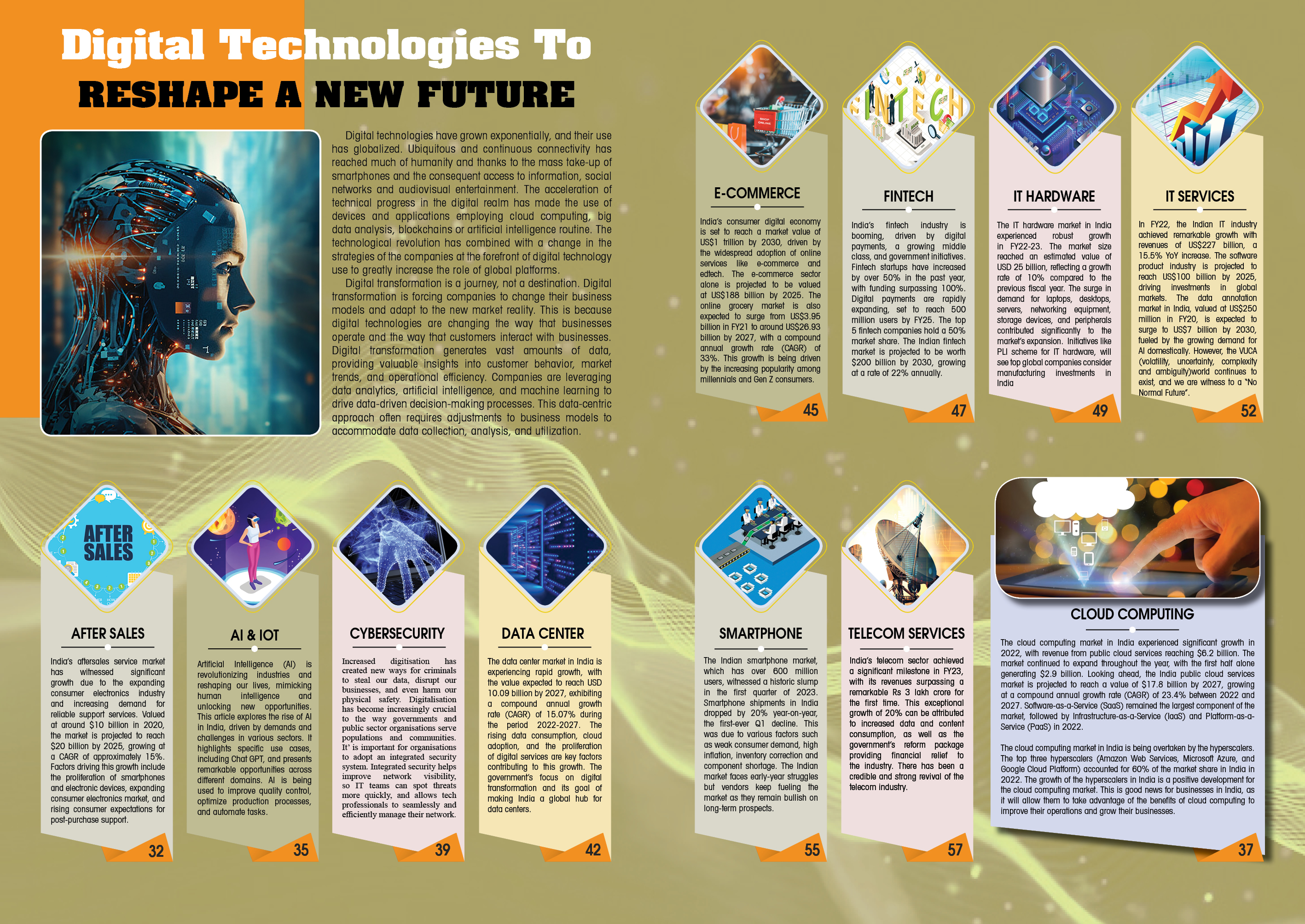
Cerebras Systems unveils 1.2 trillion transistor processor for AI
By MYBRANDBOOK

Cerebras Systems is making wafer-scale AI chips.
New artificial intelligence company Cerebras Systems is unveiling the largest semiconductor chip ever built. The Cerebras Wafer Scale Engine has 1.2 trillion transistors, the basic on-off electronic switches that are the building blocks of silicon chips. Intel's first 4004 processor in 1971 had 2,300 transistors, and a recent Advanced Micro Devices processor has 32 billion transistors. Samsung has actually built a flash memory chip, the eUFS, with 2 trillion transistors. But the Cerebras chip is built for processing, and it boasts 400,000 cores on 42,225 square millimeters.
It is 56.7 times larger than the largest Nvidia graphics processing unit, which measures 815 square millimeters and 21.1 billion transistors. The WSE also contains 3,000 times more high-speed, on-chip memory and has 10,000 times more memory bandwidth.
Most chips are actually a collection of chips created on top of a 12-inch silicon wafer and are processed in a chip factory in a batch. But the Cerebras Systems chip is a single chip interconnected on a single wafer. The interconnections are designed to keep it all functioning at high speeds so the trillion transistors all work together as one. In this way, the Cerebras Wafer Scale Engine is the largest processor ever built, and it has been specifically designed to process artificial intelligence applications. The company is talking about the design this week at the Hot Chipsconference at Stanford University in Palo Alto, California.
The WSE also contains 3,000 times more high-speed, on-chip memory and has 10,000 times more memory bandwidth. Chip size is profoundly important in AI, as big chips process information more quickly, producing answers in less time. Reducing the time to insight, or “training time,” allows researchers to test more ideas, use more data, and solve new problems.The chip comes from a team headed by Andrew Feldman, who previously founded the micro-server company SeaMicro, which he sold to Advanced Micro Devices for $334 million. Sean Lie, cofounder and chief hardware architect at Cerebras Systems, will provide an overview of the Cerebras Wafer Scale Engine at Hot Chips. The Los Altos, California company has 194 employees.
Google, Facebook, OpenAI, Tencent, Baidu, and many others argue that the fundamental limitation of today’s AI is that it takes too long to train models. Reducing training time thus removes a major bottleneck to industrywide progress.
Cerebras has designed its chip to be redundant, so one impurity won’t disable the whole chip. It has designed in so uniqueness that, “Designed from the ground up for AI work, the Cerebras WSE contains fundamental innovations that advance the state-of-the-art by solving decades-old technical challenges that limited chip size — such as cross-reticle connectivity, yield, power delivery, and packaging,” said Feldman, who cofounded Cerebras Systems and serves as CEO, in a statement. “Every architectural decision was made to optimize performance for AI work. The result is that the Cerebras WSE delivers, depending on workload, hundreds or thousands of times the performance of existing solutions at a tiny fraction of the power draw and space.”
These performance gains are accomplished by accelerating all the elements of neural network training. A neural network is a multistage computational feedback loop. The faster inputs move through the loop, the faster the loop learns, or “trains.” The way to move inputs through the loop faster is to accelerate the calculation and communication within the loop.
“Cerebras has made a tremendous leap forward with its wafer-scale technology, implementing far more processing performance on a single piece of silicon than anyone thought possible,” said Linley Gwennap, principal analyst at the Linley Group, in a statement. “To accomplish this feat, the company has solved a set of vicious engineering challenges that have stymied the industry for decades, including implementing high-speed die-to-die communication, working around manufacturing defects, packaging such a large chip, and providing high-density power and cooling. By bringing together top engineers in a variety of disciplines, Cerebras created new technologies and delivered a product in just a few years, an impressive achievement.”
With 56.7 times more silicon area than the largest graphics processing unit, Cerebras WSE provides more cores to do calculations and more memory closer to the cores so the cores can operate efficiently. Because this vast array of cores and memory is on a single chip, all communication is kept on-silicon, which means its low-latency communication bandwidth is immense, so groups of cores can collaborate with maximum efficiency.
The 46,225 square millimeters of silicon in the Cerebras WSE contains 400,000 sparse linear algebra cores, 18GB of total on-die memory, 9PB/sec worth of memory bandwidth across the chip, and separate fabric bandwidth of up to 100Pbit/sec. The entire chip is built on TSMC’s 16nm FinFET process. Because the chip is built from (most) of a single wafer, the company has implemented methods of routing around bad cores on-die and can keep its arrays connected even if it has bad cores in a section of the wafer. The company says it has redundant cores implemented on-die, though it hasn’t discussed specifics yet. Details on the design are being presented at Hot Chips this week. Cerebras WSE’s is a world record-breaking achievements would not have been possible without years of close collaboration with TSMC, the world’s largest semiconductor foundry, or contract manufacturer, and leader in advanced process technologies, the companies said. The WSE is manufactured by TSMC on its advanced 16nm process technology.
“We are very pleased with the result of our collaboration with Cerebras Systems in manufacturing the Cerebras Wafer Scale Engine, an industry milestone for wafer scale development,” said J.K. Wang, TSMC’s senior vice president of operations. “TSMC’s manufacturing excellence and rigorous attention to quality enable us to meet the stringent defect density requirements to support the unprecedented die size of Cerebras’ innovative design.”
Cores and more cores
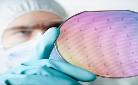
An example of a silicon wafer, which is sliced into individual chips.
The WSE contains 400,000 AI-optimized compute cores. Called SLAC for Sparse Linear Algebra Cores, the compute cores are flexible, programmable, and optimized for the sparse linear algebra that underpins all neural network computation. SLAC’s programmability ensures cores can run all neural network algorithms in the constantly changing machine learning field.
As the graphics processing units and tensor processing units are dense execution engines — engines designed to never encounter a zero — they multiply every element even when it is zero. When 50-98% of the data is zeros, as is often the case in deep learning, most of the multiplications are wasted. Imagine trying to run forward quickly when most of your steps don’t move you toward the finish line. As the Cerebras Sparse Linear Algebra Cores never multiply by zero, all zero data is filtered out and can be skipped in the hardware, allowing useful work to be done in its place.
Typical messages traverse one hardware link with nanosecond latency. The aggregate bandwidth across a Cerebras WSE is 100 petabits per second. Communication software such as TCP/IP and MPI is not needed, so their performance penalties are avoided. The energy cost of communication in this architecture is well under 1 picojoule per bit, which is nearly two orders of magnitude lower than in graphics processing units. With a combination of massive bandwidth and exceptionally low latency, the Swarm communication fabric enables the Cerebras WSE to learn faster than any currently available solutions.
"


BHIM to join e-commerce, competing with PhonePe and Google Pay
The government-supported payment software BHIM is getting ready to join t...

The latest version of X helps prevent deepfakes on social medi
To combat deepfakes and shallowfakes, Elon Musk revealed a new update t...

India and Namibia collaborate on a payment system similar to U
Once operational, the platform will enable digital transactions in Namibia,...

Sebi issues show-cause notices to six Adani group firms
Sebi issued show-cause notices to six Adani Group firms, including Adani ...


Airtel Xstream Play strengthens regional content library, part
Bharti Airtel (“Airtel”), one of India’s leading telecommunications

ED attaches Raj Kundra, Shilpa Shetty’s Rs 97 crore worth as
The Enforcement Directorate (ED) has seized businessman Raj Kundra's pro

Clover Infotech appointed Subham Banerjee as CDO
Clover Infotech has announced the appointment of Subham Banerjee as its Ch

Saviynt ropes in Sanjeevi Kumar as new Sales Director in India
The cloud-native identity and governance platform solutions provider Saviy


Dell Technologies lives by its commitment of driving growth th
Dell believes in an agile approach to innovation that leverages the brighte

Lenovo aims to solve customers' critical business needs throug
enovo recognizes the immense potential and the crucial role that technology

COLORFUL rolls out an array of gaming laptops
COLORFUL launched its incredible series of COLORFUL EVOL P15 gaming laptop

Dell Technologies launches new AI-powered commercial PC portfo
Dell Technologies has launched the broadest portfolio of commercial AI lap


SECLORE TECHNOLOGY PVT. LTD.

STERLITE TECHNOLOGIES LTD.

TP-LINK INDIA PVT LTD.

EXIDE INDUSTRIES LTD.


Technology Icons Of India 2023: Sunil Gupta
Sunil Gupta is the Co-founder, Managing Partner & CEO of Yotta Infrast...
Technology Icons Of India 2023: Amitabh Kant
Amitabh Kant is presently the G20 Sherpa of India during its Presidenc...
Technology Icons Of India 2023: Nikhil Rathi
Nikhil Rathi, Co-founder & CEO of Web Werks, a global leader in Data C...


BSE provides highly secure, efficient and transparent market for trading
BSE (formerly known as Bombay Stock Exchange Ltd.) is Asia's first & t...

C-DOT enabling India in indigenous design, development and production of telecom technologies
An autonomous telecom R&D centre of Government of India, Center of Dev...

STPI encouraging software exports from India
Software Technology Parks of India (STPI) is an S&T organization under...


TECH DATA, A TD SYNNEX COMPANY
Tech Data Corporation was an American multinational distribution compa...

NETPOLEON SOLUTIONS
Netpoleon Group is a Value-Added Distributor (VAD) of Network Security...

ADITYA INFOTECH LTD.
Aditya Infotech Ltd. (AIL) – the technology arm of Aditya Group, is ...


 Limited")